Clock Domain Fault Lines: Why Picosecond Skew at the Analog-Digital Interface Is Quietly Degrading Mixed-Signal IC Performance
The Boundary No One Is Watching Closely Enough
Every mixed-signal integrated circuit contains an implicit contract: the analog front end will sample the physical world at a precisely defined instant, and the digital back end will process that sample in strict temporal coordination. When both sides of that contract operate from perfectly aligned clocks, the system performs as the datasheet promises. When they do not, the consequences are rarely obvious—but they are almost always consequential.
The problem is not gross timing failure. Engineers have robust mechanisms for detecting and correcting clock domain crossings that produce metastability, setup violations, or outright data corruption. What evades detection far more often is the subtler category of misalignment: phase offsets measured in tens or hundreds of picoseconds between the analog sampling clock and the digital processing clock operating inside the same device. At first glance, a 50-picosecond skew between two clocks running at 100 MHz seems inconsequential. In practice, it can degrade spurious-free dynamic range (SFDR) by several decibels, introduce harmonic distortion components that were absent in simulation, and generate intermodulation products that compromise selectivity in RF receiver chains.
This is the picosecond problem, and it deserves considerably more attention than the mixed-signal design community typically gives it.
Why Analog and Digital Clocks Diverge Inside the Same IC
The architecture of a modern mixed-signal device—whether a high-speed analog-to-digital converter, a direct-conversion receiver, or a software-defined radio front end—typically distributes clocking signals across substrate regions with fundamentally different electrical characteristics. The analog domain demands low-noise, low-jitter clock delivery, often routed through dedicated shielded structures or differential clock trees designed to minimize coupling from digital switching activity. The digital domain, by contrast, is optimized for edge rate and fanout, tolerating higher noise floors in exchange for reliable logic transitions.
These two environments impose different propagation delays, different capacitive loading profiles, and different sensitivity to supply voltage transients. Even when both clocks originate from a single on-chip phase-locked loop, the routing paths to the analog sampling aperture and the digital capture register diverge almost immediately. Process variation across the die, thermal gradients driven by localized power dissipation, and substrate coupling from high-frequency digital switching all contribute to a dynamic, operating-condition-dependent skew that no static timing analysis fully captures.
The situation becomes more complex in heterogeneous integration scenarios—chiplets, multi-die packages, or system-in-package assemblies where the analog and digital functions reside on physically separate silicon. Here, the clock distribution problem crosses die boundaries, introduces bond wire or through-silicon via parasitics, and becomes sensitive to package-level thermal and mechanical stress. The nominal skew specified at room temperature and nominal supply may bear little resemblance to the actual skew encountered during full-power operation in a deployed system.
How Picosecond Skew Manifests in the Frequency Domain
The most instructive way to understand the consequences of analog-digital clock skew is to examine what it does to the sampled signal spectrum. An ideal ADC samples its input at uniformly spaced time intervals, converting the continuous analog waveform into a discrete sequence with spectral properties determined entirely by the input signal and the sampling rate. Any deviation from uniform sampling—including periodic phase modulation of the sampling clock introduced by skew coupling from the digital clock—appears in the output spectrum as spurious tones.
For a sinusoidal input at frequency f_in and a periodic skew component at frequency f_skew, the resulting spurious products appear at f_in ± f_skew and at harmonics thereof. When f_skew corresponds to the digital processing clock or its subharmonics, these spurs fall at predictable offsets from the signal of interest. In a narrowband receiver, they may land outside the channel bandwidth and be filtered. In a wideband or frequency-agile system, they become indistinguishable from legitimate signal content.
Harmonic distortion follows a similar mechanism. A systematic phase error between the analog and digital clocks that varies with signal amplitude—a nonlinear skew dependency that arises when the analog clock buffer's propagation delay is modulated by the input signal's common-mode voltage—generates harmonic components at integer multiples of f_in. This distortion mechanism is distinct from the nonlinearity of the ADC's transfer function and will not be corrected by standard harmonic distortion calibration techniques that assume a time-invariant sampling aperture.
The Limits of Standard Bench Characterization
Conventional mixed-signal test methodology measures SFDR, total harmonic distortion, and signal-to-noise-and-distortion ratio using single-tone or two-tone stimulus applied at the device input. These figures of merit are meaningful, but they are typically captured under static, steady-state conditions that do not exercise the dynamic skew mechanisms described above. The test environment supplies a low-jitter external clock, the device under test operates at a stable temperature, and the digital output is captured over a sufficiently long record to average out random noise contributions.
What this approach misses is the operating-condition sensitivity of the skew. The skew that exists when the digital back end is processing a high-activity data pattern differs from the skew present during a low-activity pattern, because digital switching current transients modulate the supply voltage seen by the analog clock buffer. A device that meets its SFDR specification under the quiescent conditions of a bench test may degrade by several decibels in a deployed system where the digital back end is running a real-time signal processing workload.
A Practical Framework for Characterizing and Tightening Interface Skew
Addressing this problem requires moving beyond static characterization toward a methodology that exposes the dynamic, operating-condition-dependent nature of analog-digital clock skew.
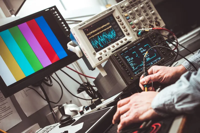
Time-interval analysis at the package boundary. Where device architecture and package pinout permit, use a high-resolution time-interval analyzer or a sampling oscilloscope with sub-picosecond timing resolution to measure the phase relationship between the analog clock reference and any accessible digital clock output under varying digital activity conditions. Systematic variation in this interval as a function of activity pattern is a direct indicator of supply-coupled skew.
Spectral stress testing with controlled digital workloads. Perform SFDR and harmonic distortion measurements while programmatically controlling the computational load on the digital back end. A device whose spectral performance is invariant across workload levels has robust isolation between its clock domains. One that shows measurable spur level variation is exhibiting the signature of dynamic skew coupling.
Supply decoupling optimization at the board level. Because supply transients are a primary coupling mechanism, the placement and value of bypass capacitors on the analog clock supply rail directly influence the magnitude of the skew. Engineers should treat analog clock supply decoupling as a timing-critical design decision, not a generic EMC measure, and validate its effectiveness through spectral testing rather than impedance simulation alone.
On-chip calibration engagement. Many high-performance ADCs and mixed-signal front ends incorporate clock phase adjustment registers or on-chip delay-locked loops specifically intended to compensate for interface skew. These features are frequently left at their default settings. Systematic characterization of the optimal phase adjustment value under representative operating conditions can recover several decibels of SFDR headroom without any additional hardware.
Closing the Gap
The analog-digital clock boundary is one of the most consequential timing interfaces in modern electronic systems, and it is chronically under-examined at the resolution it demands. As data converter speeds push into the gigasample-per-second range and mixed-signal integration density continues to increase, the picosecond-scale skew mechanisms described here will grow in significance, not diminish. Engineers who build the habit of scrutinizing this boundary with the same rigor they apply to PCB differential pair routing or PLL phase noise will find recoverable performance sitting in a domain most of their competitors have not yet learned to see.