Trace Length, Timing Death: Why Differential Pair Skew Is the Silent Killer of 100G PCB Designs
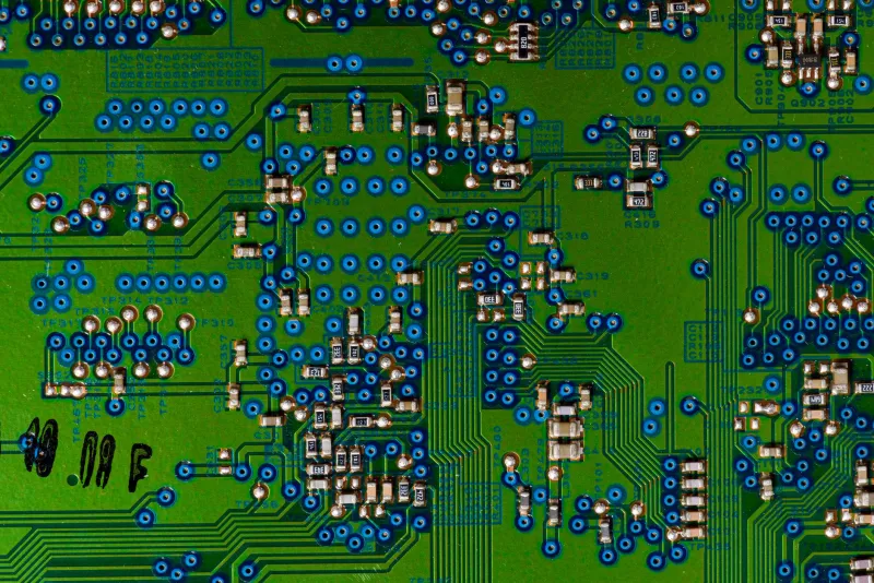
There is a particular category of engineering failure that is almost worse than an immediate, reproducible fault: the intermittent one. A 100G link that passes qualification testing, ships to a customer, and then begins dropping packets under thermal load or across manufacturing variance is the kind of failure that consumes weeks of engineering time and erodes product credibility in ways that are difficult to recover from. In a surprising number of these cases, the root cause traces back to something deceptively mundane—the physical length of copper traces on a printed circuit board.
At 100 Gbps—and increasingly at 200G and 400G as PAM4 signaling and higher-order modulation schemes become standard—timing tolerances have compressed to a domain where picoseconds are not an abstraction but a hard engineering constraint. The differential pair, long the workhorse of high-speed serial signaling precisely because of its noise immunity, becomes a liability the moment its two constituent traces diverge in electrical length by even a marginal amount. That divergence is called intra-pair skew, and it is quietly responsible for a significant fraction of production signal integrity failures that engineers initially attribute to everything else.
The Physics of Skew at High Data Rates
Differential signaling works on the principle that a receiver subtracts the negative signal from the positive signal, recovering the data while rejecting common-mode noise. This subtraction is only clean when the two signals arrive simultaneously. When they do not—when one conductor of the pair is electrically longer than the other—the signals overlap imperfectly at the receiver's input stage. The result is a reduction in differential voltage swing and, more critically, a distortion of the signal's rising and falling edges.
At 10 Gbps, the unit interval—the time window allocated to a single bit—is 100 picoseconds. At 100 Gbps using NRZ signaling, that window compresses to 10 picoseconds. A trace length mismatch of just 2.5 millimeters on a standard FR4 substrate, where signal propagation velocity runs approximately 170 picometers per picosecond, introduces roughly 15 picoseconds of skew. At 10G, that is manageable. At 100G, it consumes 150 percent of the unit interval. The eye diagram does not merely degrade—it closes entirely.
This is not a theoretical edge case. It is a routine failure mode in boards where layout engineers, under schedule pressure, allow auto-routing tools to handle differential pairs without enforcing strict length-matching rules, or where manual routing introduces serpentine meanders that look length-matched on paper but behave differently in practice.
Dielectric Variation: The Invisible Complication
Trace length matching, even when executed with precision, addresses only the geometric component of skew. Electrical length is a function of both physical length and the propagation velocity of the signal through the surrounding dielectric material. That velocity is determined by the dielectric constant—commonly called Dk or εr—of the PCB substrate.
The problem is that Dk is not uniform. In woven fiberglass substrates like FR4 and its higher-performance derivatives, the resin-rich regions between glass fiber bundles have a different dielectric constant than the fiber bundles themselves. When a differential pair's two traces are routed at slightly different angles relative to the fiber weave—a phenomenon known as fiber weave effect—they experience different average dielectric constants and therefore different propagation velocities, even if their physical lengths are identical.
This form of skew is particularly insidious because it is invisible to standard length-matching checks in EDA tools. A layout that passes design rule checks with zero length mismatch can still exhibit several picoseconds of skew due entirely to dielectric inhomogeneity. The solution involves a combination of substrate selection—materials like Megtron 6 or Rogers laminates with lower and more uniform Dk—and routing at 45-degree angles to the fiber weave rather than parallel to it, which averages out the variation across both traces in the pair.
Via Stubs and the Resonance Trap
Differential pair skew does not originate exclusively from the traces themselves. Layer transitions through vias introduce their own timing pathology, particularly through the mechanism of via stubs. When a signal transitions from one routing layer to another through a plated through-hole via, the unused portion of that via—the stub extending beyond the signal's exit layer—acts as a shunt transmission line stub. This stub creates a resonance at a frequency determined by its electrical length, and at that resonant frequency, signal energy is partially absorbed rather than transmitted.
At 100G, the fundamental Nyquist frequency is 50 GHz, and harmonics of interest extend well above that. Via stubs of even a few hundred micrometers can resonate within this range, creating notches in the channel's insertion loss profile that degrade specific frequency components of the signal and, in the time domain, manifest as inter-symbol interference and eye closure that shifts with temperature as the stub's electrical length changes.
The engineering remedies include back-drilling—mechanically removing the stub after board fabrication—and the use of blind or buried vias that eliminate the stub entirely. Both approaches add cost and manufacturing complexity, which is why the decision to implement them must be driven by rigorous pre-layout simulation rather than post-production firefighting.
Simulation Before Copper: The Only Viable Strategy
The density of interacting failure mechanisms at 100G—geometric skew, dielectric variation, via stubs, impedance discontinuities at connector launches—makes post-layout debugging an exercise in diminishing returns. By the time a board has been fabricated and assembled, the cost of respinning to correct a routing problem is substantial, and the diagnostic process of isolating which mechanism is responsible for an observed eye diagram failure is enormously time-consuming.
The signal integrity discipline has responded by moving simulation upstream. Channel modeling tools such as Ansys SIwave, Cadence Clarity, and Keysight ADS allow engineers to build full electromagnetic models of critical differential pairs before layout is committed to fabrication. These tools can extract S-parameters for entire channel segments including vias, connectors, and package launches, and feed those parameters into time-domain channel simulations that predict eye diagram quality with reasonable accuracy.
The key practice is to simulate not just the nominal design but a statistical distribution of manufacturing variations—Dk tolerance, trace width variation from etching, via drill registration error—to understand how yield will behave across a production population. A design that produces a marginal eye diagram at nominal conditions will produce a failing one at the edges of the manufacturing distribution.
Measurement: Closing the Loop Between Model and Reality
Simulation is necessary but not sufficient. Correlating electromagnetic models with physical measurements is how signal integrity engineers validate their assumptions and improve model accuracy for future designs. Time-domain reflectometry remains the fundamental measurement technique for characterizing impedance discontinuities along a differential channel, identifying the precise location of stub resonances and routing asymmetries with sub-millimeter spatial resolution.
Vector network analyzer measurements of differential S-parameters—specifically SDD21 for insertion loss and SDD11 for return loss—provide frequency-domain characterization that, when transformed via inverse FFT, yields time-domain impulse responses that can be directly compared against simulation output. Discrepancies between measured and simulated responses point to modeling assumptions that require refinement, most commonly around via geometry or dielectric constant values that differ from the manufacturer's nominal specification.
At 100G and beyond, the picosecond is no longer a unit reserved for laboratory physics. It is a practical engineering tolerance that determines whether a product ships or fails. The teams that internalize this—that treat trace routing as a timing problem governed by electromagnetic physics rather than a geometric layout task—are the ones building designs that survive contact with production reality.