Timing Uncertainty Unpacked: A Systematic Guide to Jitter Classification and Suppression in High-Speed Digital Links
In high-speed digital design, few phenomena are as pervasive, as consequential, or as frequently misdiagnosed as jitter. Timing uncertainty accumulates quietly across a signal path—introduced by oscillators, amplified by transmission line discontinuities, compounded by crosstalk—until the system begins exhibiting errors that appear random but are, in fact, deterministic in origin. Understanding jitter at a fundamental level is not optional for engineers working on PCIe Gen 4 and Gen 5 links, USB 3.x implementations, SERDES-based communications, or high-resolution medical imaging systems. It is a prerequisite for shipping hardware that works.
This guide establishes a clear taxonomy, reviews measurement approaches used in professional US laboratory settings, and surveys the mitigation strategies that have proven most effective in practice.
Defining the Problem: What Jitter Actually Is
Jitter is the deviation of a signal's edge transitions from their ideal positions in time. In an ideal digital system, every rising and falling edge would occur at precisely the moment dictated by the clock or data encoding scheme. In practice, edges arrive early or late due to a variety of physical mechanisms, and that temporal displacement—measured in picoseconds or femtoseconds at the extremes of modern high-speed design—determines whether a receiver samples a bit correctly or misinterprets it.
The consequences scale with data rate. At 1 Gbps, a unit interval is 1 nanosecond, and a few hundred picoseconds of jitter may be tolerable. At 32 Gbps, the unit interval shrinks to approximately 31 picoseconds. Jitter that would have been inconsequential at lower speeds now consumes a substantial fraction of the available timing budget, leaving little margin for other contributors.
The Jitter Taxonomy
The signal integrity community has converged on a hierarchical decomposition of jitter that is essential for both diagnosis and mitigation. The top-level distinction is between Total Jitter (TJ) and its constituent components.
Random Jitter
Random jitter (RJ) is stochastic in nature, arising primarily from thermal noise in active devices, shot noise in semiconductor junctions, and phase noise in oscillator circuits. Its amplitude distribution is Gaussian, which means it has no theoretical upper bound—only a probability of occurrence at any given magnitude. This characteristic makes RJ particularly problematic for systems requiring very low bit error rates, because the tails of the Gaussian distribution extend into regions that, while improbable, are not impossible.
In practice, RJ is quantified by its RMS value and extrapolated to a target BER using Q-factor analysis. Reducing RJ typically requires improving the noise floor of the clock source, optimizing power supply rejection in clock distribution circuits, or selecting lower-noise oscillator components.
Deterministic Jitter
Deterministic jitter (DJ) is bounded and repeatable. Unlike RJ, it has identifiable causes and predictable amplitude limits, which means it can, in principle, be eliminated if its source is identified. DJ is further subdivided into several categories.
Periodic jitter (PJ) appears as sinusoidal or otherwise regular modulation of edge timing, typically caused by power supply noise at a specific frequency coupling into the clock path, or by electromagnetic interference from a nearby switching regulator or digital bus. PJ is often visible as sidebands in the phase noise spectrum of a clock signal.
Data-dependent jitter (DDJ), also called intersymbol interference (ISI), arises when the transition history of a data stream influences the timing of subsequent edges. It is caused by the frequency-dependent loss characteristics of transmission media—PCB traces, cables, and connectors all attenuate high-frequency content more aggressively than low-frequency content, causing the waveform to retain a memory of past symbols. DDJ is a primary concern in NRZ-coded links and grows more severe as channel loss increases.
Duty cycle distortion (DCD) manifests as a systematic difference in the duration of positive and negative half-cycles, often introduced by asymmetries in driver output characteristics or by single-ended to differential conversion circuits.
Bounded uncorrelated jitter (BUJ) covers deterministic contributions that do not correlate with the data pattern, such as crosstalk from adjacent aggressor signals. It is bounded in amplitude but not predictable from the victim signal alone.
Measurement Methodologies
Accurate jitter measurement requires both appropriate instrumentation and a clear understanding of what each measurement approach actually captures.
Time-Interval Analysis
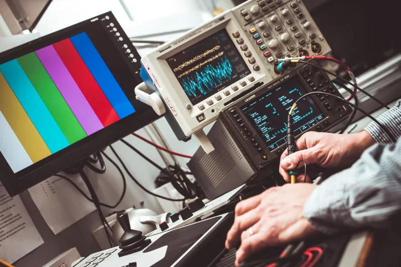
The most direct approach uses a high-resolution oscilloscope or time-interval analyzer to capture edge arrival times over a large number of cycles, then compute the statistical distribution of deviations from the ideal period. Modern sampling oscilloscopes from vendors such as Keysight, Tektronix, and Rohde & Schwarz offer timing resolution in the femtosecond range, enabling sub-picosecond jitter characterization on recovered clock signals.
For this technique to yield meaningful results, the trigger jitter of the instrument must be well below the jitter being measured. Equivalent-time sampling oscilloscopes are generally preferred for very high-frequency signals because they achieve superior vertical and timing resolution compared to real-time instruments at equivalent bandwidth.
Spectrum-Based Phase Noise Analysis
Phase noise measurement using a signal source analyzer provides a frequency-domain view of clock jitter. The integrated phase noise over a specified offset frequency range converts directly to RMS jitter, making this approach particularly useful for characterizing oscillators and PLLs. This method is standard practice in US RF and microwave engineering labs and is specified in many system-level jitter budgets.
Eye Diagram Analysis
The eye diagram remains the most widely used tool for evaluating the cumulative effect of jitter in a data link. By overlaying thousands of bit periods on a single display, the eye diagram renders timing margin visually as the horizontal opening of the eye. Automated jitter decomposition software, available on most modern oscilloscopes, fits statistical models to the measured eye to separate RJ from DJ components—a process known as jitter separation or jitter decomposition.
Bathtub curves, derived from eye diagram measurements, plot the BER as a function of sampling point across the unit interval and are required for compliance testing on standards including PCIe, USB, and SATA.
Mitigation Strategies
Spread-Spectrum Clocking
Spread-spectrum clocking (SSC) intentionally modulates the clock frequency over a small range—typically ±0.5% for PCIe—at a low modulation rate. This spreads the spectral energy of the clock across a wider frequency range, reducing peak EMI emissions. SSC does introduce additional jitter as a side effect, specifically a form of periodic jitter synchronized to the modulation frequency, and downstream receivers must be designed to tolerate it. SSC is disabled in applications where absolute timing precision is required, such as synchronous networking.
Impedance Matching and Transmission Line Discipline
DDJ caused by channel loss is most effectively addressed at the physical layer through careful impedance control. Maintaining consistent trace impedance—typically 50 ohms for single-ended and 100 ohms differential for high-speed serial links—minimizes reflections that distort edge timing. Via stubs, impedance discontinuities at connectors, and reference plane splits are common sources of DDJ that are entirely preventable through disciplined PCB layout practice.
Equalization techniques, including both transmit-side pre-emphasis and receive-side continuous-time linear equalization (CTLE) or decision feedback equalization (DFE), compensate for frequency-dependent channel loss and are now standard in SERDES implementations at data rates above 10 Gbps.
Phase-Locked Loop Optimization
The PLL is both a jitter filter and a potential jitter source. A PLL's loop bandwidth determines which input jitter components are tracked and which are rejected. A wide loop bandwidth tracks high-frequency input jitter, passing it to the output; a narrow loop bandwidth attenuates high-frequency input noise but makes the output more susceptible to VCO phase noise at low offset frequencies. Optimizing loop bandwidth for a given application requires characterizing both the input reference noise and the VCO noise floor, then selecting a crossover point that minimizes total integrated phase noise.
Building a Jitter Budget
Effective jitter management begins at the architecture stage, not during debug. A jitter budget allocates the available timing margin across all contributors—clock source, distribution network, transmission channel, and receiver—and establishes maximum allowable values for each. Maintaining a living jitter budget throughout the design process ensures that margin is not inadvertently consumed by incremental decisions that each seem individually acceptable.
For engineers working within the constraints of established US industry standards, compliance specifications such as those published by the PCI-SIG, USB Implementers Forum, and JEDEC provide the outer bounds of the jitter budget and define the measurement conditions under which compliance is evaluated.
Jitter is not an abstraction. It is a physical phenomenon with traceable causes, measurable characteristics, and tractable solutions. Approaching it systematically—from taxonomy through measurement to mitigation—is the discipline that separates designs that merely function from designs that perform reliably at the margins where it matters most.